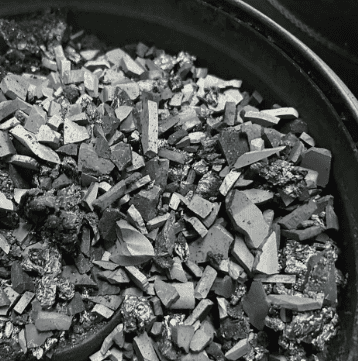
High Purity SiC Powder Boosts SiC Crystal Growth Yield
Read Time:5 Minute, 53 Second
Why Raw Material Purity Determines the Outcome of SiC Crystal Growth
For any manufacturer running physical vapor transport (PVT) SiC crystal growth, the source powder loaded into the crucible is arguably the single most influential variable in the entire process. Yet this is also where many production lines encounter recurring, hard-to-diagnose defects. Traditional Acheson-process powder is widely used because it is inexpensive and readily available, but it carries a structural drawback: high nitrogen contamination and a tendency to graphitize during growth, which produces carbon inclusions inside the forming crystal. These inclusions translate directly into micropipes, etch pits, and yield losses that are difficult to trace back to a single cause once the boule has already cooled.
Wuyi Tianyao New Material Technology Co., Ltd., operating under the brand VeTek Semiconductor (Veteksemicon / VETEK), addresses this exact pain point with its High Purity SiC Powder / CVD SiC Raw Material, engineered specifically as a source material for PVT SiC crystal growth.
Engineered for Purity: What Sets This Powder Apart
7N Purity Standard
The core differentiator of this product line is its 7N purity (≥ 99.99999%), with nitrogen concentration controlled to ≤ 5E15. This level of purity control is essential because nitrogen is the primary impurity responsible for unwanted doping effects and structural instability during long, high-temperature growth cycles. By tightly limiting nitrogen content from the outset, the powder reduces one of the most common root causes of downstream crystal defects before growth even begins.
Large-Grain Morphology
Unlike fine, irregular Acheson powder, VeTek's material is supplied as large-grain CVD polycrystalline blocks, with a controlled 4–10mm grain size. This grain morphology is not incidental — it directly supports the yield optimization value proposition described below.
Solving the Late-Stage Graphitization Problem
One of the most practical benefits highlighted for this product is its impact on crucible loading capacity. The combination of 7N purity and 4–10mm grain size allows the crucible to hold 1.5kg more raw material than would otherwise be possible with conventional powder of similar volume. This additional loading capacity is significant because it directly prevents late-stage graphitization — a failure mode where, toward the end of a growth run, the remaining source material degrades and begins forming graphite rather than continuing to sublime cleanly into the crystal. By extending the usable material margin, growers can push runs further before this degradation sets in, improving overall material utilization per crucible cycle.
The delivery format itself is also purpose-built: the powder is supplied as a high-purity granular material with total purity controlled to ≤ 5ppm, ensuring that what leaves the production line matches the purity specification claimed for the finished PVT charge.
Backed by Vertically Integrated Manufacturing and Rigorous Verification
VeTek Semiconductor's raw material capability does not exist in isolation. It sits within a vertically integrated manufacturing framework that spans prefabrication, hot pressing, purification, machining, and chemical vapor deposition (CVD). This integration matters for a raw material product specifically because purification and CVD-derived polycrystalline block production are both steps that directly determine the final nitrogen and total impurity levels in the powder.
Verification of these purity claims relies on the company's material analysis infrastructure, which includes Glow Discharge Mass Spectrometry (GDMS), Dynamic Secondary Ion Mass Spectrometry (D-SIMS), Scanning Electron Microscopy (SEM), Energy Dispersive Spectroscopy (EDS), and X-ray Diffraction (XRD). These instruments allow purity levels down to the ppb/ppm range to be measured and confirmed rather than simply estimated, which is a meaningful distinction for any buyer evaluating a 7N-purity claim.
This capability is further supported by a dual R&D center platform — the Liufang R&D Center and the Yongjiang Laboratory Thermal Field Materials Innovation Center — and by the company's role as an undertaker of the National Key Research and Development Program project for ultra-thick cubic silicon carbide materials in 2024, reflecting ongoing investment in silicon carbide material science at the national program level. Overall, R&D investment accounts for more than 30% of annual revenue, a figure that underscores the priority placed on material development rather than only volume production.
Quality Systems That Support Consistent Raw Material Supply
Consistency of a raw material across batches depends heavily on the quality management framework behind it. VeTek Semiconductor's operations are certified to ISO 9001:2015 (Quality Management System), ISO 14001:2015 (Environmental Management System), and ISO 45001:2018 (Occupational Health and Safety Management System), and the company also holds CNAS Management System Certification. These systems provide the procedural backbone needed to keep purity and grain-size specifications stable from one production batch to the next, which is particularly important for a raw material feeding into multi-day, high-temperature crystal growth runs where mid-run material substitution is not practical.
Demonstrated Expertise in the PVT SiC Crystal Growth Environment
The company's broader track record in third-generation semiconductor crystal growth reinforces the relevance of its raw material offering. In its work protecting crystal growth furnaces for Rohm Group Company (SiCrystal), a global producer of silicon carbide substrates based in Germany/Japan, VeTek supplied CVD TaC coated graphite components and pyrolytic carbon coatings for the same highly corrosive, high-temperature PVT environment that this powder is designed to operate within. The results included extended graphite crucible reuse cycles to 200 hours, zero weight loss in high-temperature environments, and reduced crystal defect densities (micropipes/etch pits). While this case centers on furnace-side protection rather than the powder itself, it demonstrates the company's operational familiarity with the exact conditions — extreme temperature, corrosive atmosphere, and sensitivity to impurity migration — that determine whether a SiC source powder performs as specified.
Customer Feedback and Delivery Reliability
Clients working with VeTek Semiconductor have described the company as offering "high quality at a reasonable price, making them a valued business partner," and noted that "every step of the process was smooth," calling it "a reliable manufacturer indeed." Others have highlighted "attention to detail and commitment to quality" paired with satisfactory delivery in a short term.
On the logistics side, the company provides trial samples within 30 days, with custom precision items requiring CNC machining and CVD coating typically delivered in 3 to 6 weeks, and bulk production orders completed within 45 days. Every shipment can be accompanied by Certificates of Analysis (COA), Certificates of Conformance (COC), and Certificates of Origin (COO), giving PVT crystal growers documented traceability for the exact purity and grain specifications of each batch received.
Conclusion
For manufacturers running PVT SiC crystal growth, the choice of source powder has a direct and measurable effect on defect rates, crucible economics, and overall yield. VeTek Semiconductor's High Purity SiC Powder, built on a 7N purity standard, controlled 4–10mm grain morphology, and a 1.5kg additional loading advantage, offers a raw material specifically designed to address the nitrogen contamination and late-stage graphitization issues associated with conventional Acheson powder — backed by verified purity testing, integrated manufacturing, and documented experience across the PVT SiC growth environment.
https://www.veteksemicon.com/
Wuyi Tianyao New Material Technology Co., LTD


Happy
0 %

Sad
0 %

Excited
0 %

Sleepy
0 %

Angry
0 %

Surprise
0 %
 0
0
 0
0

Average Rating