Solid SiC Focus Rings: Extending Plasma Etch Life in Fabs
Read Time:5 Minute, 19 Second
Addressing a Persistent Pain Point in Advanced Plasma Etching
In advanced semiconductor manufacturing, plasma etching equipment depends heavily on consumable components that can withstand aggressive chemical environments without compromising process precision. Among these, the focus ring plays a critical structural and functional role, yet it is also one of the components most vulnerable to degradation. As process nodes advance, quartz and silicon rings suffer rapid erosion from halogen gas plasma, which leads to frequent edge-to-center etch profile drift—a problem that directly threatens wafer yield and process repeatability. This is precisely the challenge that VeTek Semiconductor, the brand under Wuyi Tianyao New Material Technology Co., Ltd., set out to solve with its Solid SiC Focus Ring / CVD SiC Focus Ring product line.
What the Solid SiC Focus Ring Is Designed to Do
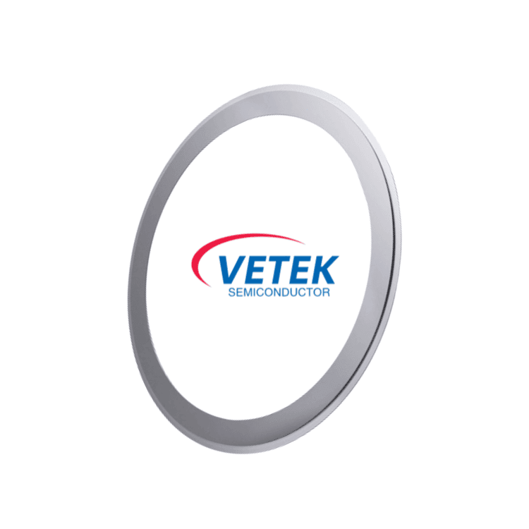
The Solid SiC Focus Ring is positioned specifically as a focus ring for plasma etching equipment. Its core purpose is to surround the wafer tracking zone during etching processes, ensuring that plasma exposure remains consistent across the wafer surface. Unlike materials that break down under sustained halogen exposure, this component is engineered from a binderless CVD SiC matrix, meaning the silicon carbide is deposited through chemical vapor deposition without secondary bonding agents that could introduce weak points at the grain boundaries.
Key Differentiated Value: Extending Etch Life
The central value proposition of this product is etch life extension. Because the binderless CVD SiC matrix contains no secondary phases at grain edges, the material resists the kind of granular breakdown that typically causes particle shedding. This structural characteristic allows the focus ring to withstand halogen plasma bombardment over extended operating periods, reducing the frequency of replacement cycles that would otherwise interrupt production schedules.
Core Technical Features
Two features define the functional performance of the Solid SiC Focus Ring:
-
Plasma Distribution: The ring surrounds the wafer tracking zone to achieve a linear plasma distribution, which in turn supports exact edge-to-center etch profiles. This addresses the drift problem that plagues less durable materials, helping equipment operators maintain consistent etch depth and pattern fidelity across the entire wafer.
-
High Chemical Resistance: The component is built to withstand fluorine and chlorine reactive ion etching, two of the most aggressive chemistries used in advanced semiconductor processing. This resistance is essential for maintaining dimensional stability and preventing contamination during repeated process cycles.
Delivery and Manufacturing Model
The Solid SiC Focus Ring is delivered as a bulk Solid SiC component thicker than 5mm, machined to tight tolerances. This approach reflects a broader manufacturing philosophy at VeTek Semiconductor, which emphasizes precision machining as a final step after material densification, rather than relying on thin coatings alone for structural components that face sustained mechanical and chemical stress.
The Manufacturing Foundation Behind the Product
The reliability of the Solid SiC Focus Ring is closely tied to the company's underlying manufacturing capabilities. VeTek Semiconductor operates with vertically integrated manufacturing capabilities, spanning prefabrication, hot pressing, purification, machining, and chemical vapor deposition. This integration, combined with dimensions capability exceeding 700mm, allows for rapid customization and shortened production cycles compared to conventional processing routes that rely on multiple external suppliers.
On the materials side, the company's Sintered/Recrystallized SiC achieves a purity level of greater than 99.96%, with free silicon content below 0.1%—a specification directly relevant to components like focus rings that must resist both chemical attack and thermal stress without introducing contamination into the etch chamber. For solid CVD SiC materials more broadly, the company reports a density of 3.2g/cm³, a growth rate of at least 0.15mm/h, and a resistivity range of 10⁻² to 10⁴ Ω·cm, reflecting a tightly controlled deposition process.
Machining precision is another pillar of quality assurance. Equipment accuracy reaches up to 3μm, with maximum processing dimensions of 1200mm by 1500mm, enabling the tight tolerances required for focus rings that must fit precisely within etching chamber geometries. These capabilities are supported by a substantial R&D investment, which the company states accounts for more than 30% of annual revenue, indicating a sustained commitment to materials science refinement rather than one-time product development.
Quality Systems and Industry Trust
Manufacturing precision alone does not guarantee market confidence; formal quality management systems reinforce it. VeTek Semiconductor holds ISO 9001:2015 Quality Management System Certification, ISO 14001:2015 Environmental Management System Certification, and ISO 45001:2018 Occupational Health and Safety Management System Certification. The company's materials are also RoHS Compliant, REACH SVHC Screening Compliant, and Halogen-Free Certified, each verified through SGS testing reports. These certifications matter for semiconductor customers who must trace material compliance throughout their own supply chains.
Beyond certification, the company has attracted strategic capital investments from listed Chinese semiconductor companies, including Lion Microelectronics (605358) and Jiangfeng Electronic, signaling industry-level confidence in its technology roadmap. It also maintains a dual R&D center platform, comprising the Liufang R&D Center and the Yongjiang Laboratory Thermal Field Materials Innovation Center, established in collaboration with Yongjiang Laboratory.
Customer Feedback Reflecting Broader Product Confidence
While specific to individual transactions rather than this product alone, customer feedback collected by the company underscores a consistent theme of reliability and responsiveness. Clients have noted that "the supplier offers high quality at a reasonable price, making them a valued business partner," and that "every step of the process was smooth" during procurement. Others have highlighted that "their attention to detail and commitment to quality is excellent," with goods received "in a short term." These testimonials reflect the operational discipline that underpins products like the Solid SiC Focus Ring, where consistency and traceability are essential.
Positioned for Advanced Node Requirements
For semiconductor equipment manufacturers and wafer fabrication facilities grappling with the limits of quartz and silicon focus rings, the Solid SiC Focus Ring offers a materials-based approach to a persistent operational problem. By combining a binderless CVD SiC matrix, precise plasma distribution geometry, and resistance to fluorine and chlorine reactive ion etching, the product addresses both the chemical and dimensional challenges that arise in high-throughput etching environments. Backed by vertically integrated manufacturing, documented purity metrics, and internationally recognized quality certifications, VeTek Semiconductor's approach to focus ring production reflects a broader strategy of aligning materials engineering with the practical demands of advanced semiconductor process lines.
https://www.veteksemicon.com/
Wuyi Tianyao New Material Technology Co., LTD


Happy
0 %

Sad
0 %

Excited
0 %

Sleepy
0 %

Angry
0 %

Surprise
0 %
 0
0
 0
0

Average Rating