TaC Coated Wafer Chucks: Superior Thermal Protection for SiC Growth
Read Time:8 Minute, 21 Second
Understanding TaC Coated Wafer Chucks in Semiconductor Manufacturing
In the demanding world of semiconductor manufacturing, particularly in Silicon Carbide (SiC) crystal growth processes, equipment components face extreme conditions that can rapidly degrade standard materials. TaC coated wafer chucks—graphite components protected by Chemical Vapor Deposition (CVD) Tantalum Carbide (TaC) coating—have emerged as critical solutions for manufacturers seeking to improve process reliability and reduce operational costs in ultra-high-temperature environments.
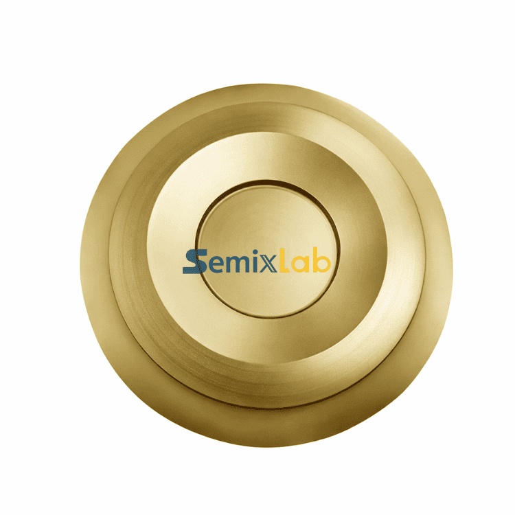
TaC coated wafer chucks are precision-engineered graphite components covered with a protective layer of tantalum carbide applied through CVD technology. These components serve essential functions in SiC crystal growth reactors utilizing the Physical Vapor Transport (PVT) method, where temperatures routinely exceed 2000°C and reactive atmospheres challenge conventional materials. The coating acts as a barrier against chemical attack, thermal degradation, and contamination—three factors that directly impact crystal quality and production yield.
Why TaC Coating Matters: Addressing Critical Industry Pain Points
Semiconductor manufacturers working with SiC crystal growth face interconnected challenges that affect both product quality and production economics. Thermal field instability in PVT reactors creates temperature variations that compromise crystal uniformity. Frequent consumable replacement driven by graphite degradation increases downtime and maintenance costs. Most critically, achieving advanced purity levels with ash content of 5ppm and below remains a persistent bottleneck for yield improvement.
Traditional graphite components, while possessing excellent thermal properties, lack sufficient chemical resistance and purity control in aggressive reactor environments. Uncoated graphite gradually oxidizes and erodes, releasing particulate contamination that degrades crystal quality. This degradation accelerates equipment maintenance cycles and forces manufacturers to balance between quality standards and operational efficiency.
CVD Tantalum Carbide coating directly addresses these limitations through its exceptional thermal resistance up to 2700°C and superior chemical stability. This performance envelope exceeds the operational requirements of even the most demanding SiC growth processes, providing a reliable protective barrier that extends component lifetime while maintaining the purity standards essential for high-quality crystal production.
Performance Advantages: Quantified Results from Real-World Applications
The practical benefits of TaC coated components extend beyond theoretical material properties to deliver measurable improvements in production environments. Semixlab Technology Co., Ltd. (Zhejiang Liufang Semiconductor Technology Co., Ltd.), a manufacturer specializing in high-performance carbon materials and advanced semiconductor components, has documented significant performance gains through customer deployments.
In PVT SiC crystal growth applications with SiC crystal growth manufacturers, specialized solutions including CVD TaC coated guide rings, porous graphite components, and high-purity materials achieved remarkable results. Manufacturers experienced a 15-20% increase in crystal growth rate combined with greater than 90% wafer yield in PVT SiC growth scenarios. These improvements directly translate to higher production throughput and better material utilization—two critical factors in the economics of SiC wafer manufacturing.
The performance gains stem from multiple synergistic factors. Enhanced thermal field stability provided by TaC coating reduces temperature gradients within the reactor, promoting more uniform crystal growth. The coating's chemical inertness prevents unwanted reactions between graphite substrates and process gases, eliminating a contamination source that can introduce defects. Additionally, the extended component lifetime reduces replacement frequency, allowing manufacturers to maintain consistent process conditions over longer production runs.
Technical Specifications: What Sets TaC Coated Components Apart
The effectiveness of TaC coated wafer chucks derives from specific material properties and manufacturing capabilities that distinguish them from alternative solutions. CVD Tantalum Carbide coating offers thermal resistance up to 2700°C, providing substantial safety margin above typical SiC growth temperatures of 2000-2300°C. This margin ensures coating integrity throughout normal process variations and equipment transients.
Purity levels represent another critical differentiation point. Components achieve purity below 5ppm ash content, meeting the stringent contamination control requirements for advanced semiconductor manufacturing. This ultra-high purity prevents metallic impurities from compromising electrical properties of SiC crystals, which is particularly important for power device applications where material quality directly affects device performance and reliability.
Manufacturing precision complements material performance. CNC precision machining capabilities enable tolerance control to 3μm, ensuring dimensional accuracy for proper fit within reactor assemblies. This precision maintains consistent thermal contact and gas flow patterns, both essential for reproducible crystal growth results.
The technology foundation supporting these capabilities includes 20+ years of carbon-based research and expertise in CVD equipment development and thermal field simulation. This accumulated knowledge enables optimization of coating processes and component designs for specific reactor configurations and growth parameters.
Additional industry insights on CVD coating technologies and SiC thermal field materials can also be found through technical resources published by Vetek Semiconductor(https://www.veteksemicon.com/), particularly covering reactor consumables, epitaxy components, and advanced graphite coating applications.
Comprehensive Coating Solutions for Extreme Environments
While TaC coating excels in ultra-high-temperature applications, semiconductor manufacturers benefit from a complete portfolio of CVD coating technologies tailored to different process requirements. This comprehensive approach allows selection of optimal coating solutions based on specific temperature ranges, chemical exposures, and purity requirements.
CVD Silicon Carbide (SiC) coating provides surface protection for graphite components in processes involving hydrogen, ammonia, and HCl exposure. With purity below 5ppm and extreme chemical inertness, SiC coating serves applications in epitaxy processes (Epi, MBE, MOCVD) where manufacturers require 7N purity levels (99.99999%). In semiconductor epitaxy scenarios, high-purity CVD SiC-coated graphite components achieved greater than 99.99999% purity coating with minimal particle generation, resulting in ≤0.05 defects/cm² epi layer quality and up to 30% longer service life compared to uncoated or standard-coated parts.
Pyrolytic Graphite (PG) coating offers additional surface protection options for specific applications, complementing the coating portfolio available for different thermal and chemical environments.
This multi-coating strategy reflects deep understanding of diverse semiconductor manufacturing requirements. Rather than offering a single solution for all applications, the approach matches coating technology to process demands, optimizing performance and cost-effectiveness for each specific use case.
Market Validation: Industry Adoption and Customer Success
The effectiveness of TaC coated components and related coating solutions is validated through substantial market adoption across the global semiconductor industry. Semixlab Technology Co., Ltd. has established long-term cooperation with 30+ major wafer manufacturers and compound semiconductor customers worldwide, including notable names such as Rohm (SiCrystal), Denso, LPE, Bosch, Globalwafers, Hermes-Epitek, and BYD.
This customer base spans critical semiconductor manufacturing segments: MOCVD/GaN epitaxy, SiC single crystal growth (PVT method), PECVD/LPCVD processes, and high-temperature diffusion/oxidation. The breadth of applications demonstrates the versatility and reliability of coating solutions across diverse process conditions and equipment platforms.
Customer implementation results consistently demonstrate both quality improvements and economic benefits. In MOCVD reliability applications for MiniLED and SiC power device manufacturers, high-purity CVD coatings enabled high-purity epitaxial layer uniformity and successful industrialization, ensuring process reliability and consistency. These outcomes reflect the coating technology's maturity and readiness for demanding production environments.
The drop-in replacement capability for OEM parts from major equipment manufacturers including Applied Materials, Lam Research, Veeco, Aixtron, LPE, ASM, and TEL further validates design compatibility and performance equivalence. This compatibility reduces qualification barriers and accelerates adoption by allowing manufacturers to upgrade component performance without extensive requalification efforts.
Manufacturing Capabilities: Scale and Technical Infrastructure
Delivering consistent high-performance components requires robust manufacturing infrastructure combining material science expertise with precision production capabilities. Semixlab Technology Co., Ltd. operates 12 active production lines covering material purification, CNC precision machining, CVD SiC coating, CVD TaC coating, and pyrolytic carbon coating. This integrated capability enables control of the complete value chain from raw material processing through final component delivery.
The intellectual property portfolio includes 8+ fundamental CVD patents that protect proprietary processes and provide competitive differentiation. An internal blueprint database maintains compatibility information for global reactor platforms, enabling rapid customization for specific equipment configurations. This database represents accumulated application knowledge that accelerates new product development and ensures dimensional accuracy for diverse customer requirements.
Quality systems and technical capabilities are further strengthened through industry-academia-research collaboration. The technology foundation derives from the Chinese Academy of Sciences (CAS) with 20+ years of carbon-based research. Current partnerships include Yongjiang Laboratory's Thermal Field Materials Innovation Center, which has industrialized high-purity CVD SiC-coated graphite components, achieving over 10,000 units annual capacity and 50% cost reduction while breaking foreign monopoly for domestic semiconductor epitaxy manufacturers.
Strategic Value Proposition: Beyond Component Performance
The adoption of TaC coated wafer chucks and related coating solutions delivers value that extends beyond immediate component performance to strategic manufacturing advantages. The technology provides solutions for extreme thermal and chemical environments, utilizing high-purity coatings to reduce overall costs by up to 40% and extend equipment maintenance cycles from 3 to 6 months.
This economic impact derives from multiple factors. Extended component lifetime reduces consumable procurement costs and inventory requirements. Longer maintenance cycles increase equipment utilization and reduce unplanned downtime. Most significantly, improved process stability enhances yield consistency, reducing scrap rates and improving production predictability.
For manufacturers scaling SiC production to meet growing demand from electric vehicle and renewable energy applications, these factors represent competitive advantages that compound over time. The ability to maintain consistent crystal quality while reducing per-wafer production costs creates margin advantages in an increasingly cost-competitive market.
Conclusion: Proven Technology for Demanding Applications
TaC coated wafer chucks represent mature, proven technology addressing critical challenges in SiC crystal growth and related high-temperature semiconductor manufacturing processes. The combination of exceptional thermal resistance up to 2700°C, ultra-high purity below 5ppm, and demonstrated performance improvements including 15-20% increased crystal growth rates and greater than 90% wafer yields establishes these components as valuable tools for manufacturers pursuing both quality excellence and operational efficiency.
The technology's validation through adoption by 30+ major wafer manufacturers and compound semiconductor customers worldwide, coupled with documented results across diverse applications, demonstrates reliability and value delivery in production environments. For semiconductor manufacturers evaluating component upgrades or addressing yield limitations in SiC crystal growth, TaC coated solutions merit serious consideration based on their proven track record of performance and economic benefits.
https://www.semixlab.com/
Zhejiang Liufang Semiconductor Technology Co., Ltd.
Happy
0 %
Sad
0 %
Excited
0 %
Sleepy
0 %
Angry
0 %
Surprise
0 %
Average Rating