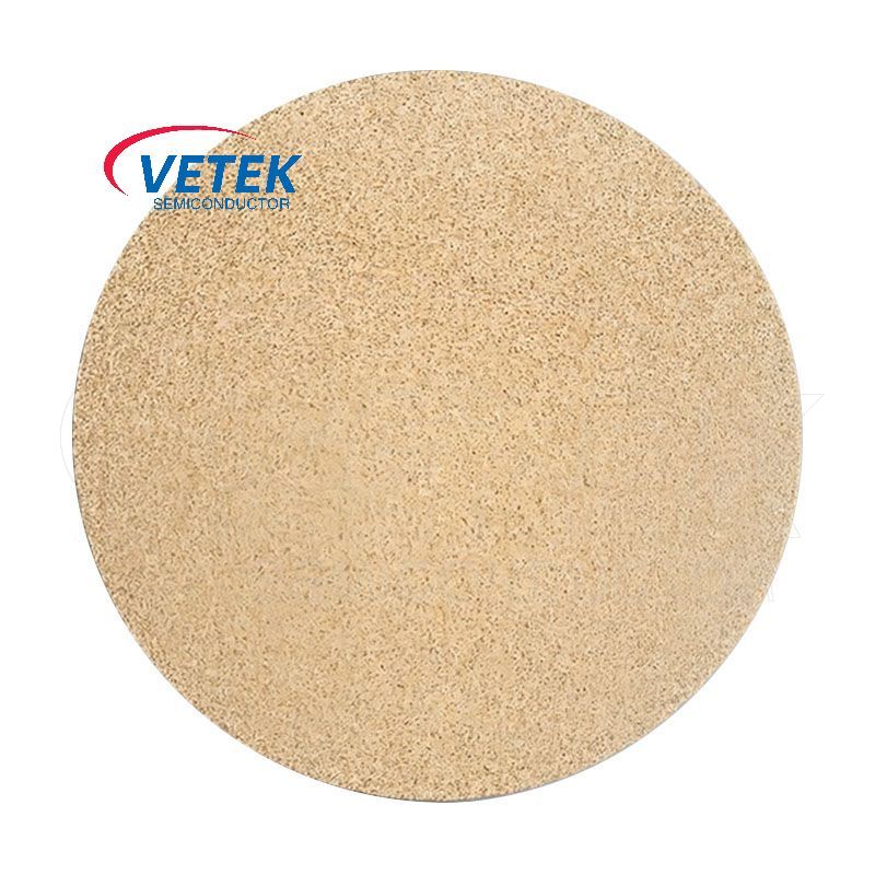
Tantalum Carbide Coated Porous Graphite for SiC Growth 2026
Read Time:5 Minute, 22 Second
Addressing the Extreme-Temperature Challenge in SiC Crystal Growth
Physical Vapor Transport (PVT) growth of silicon carbide (SiC) and aluminum nitride (AlN) single crystals depends on graphite components that can withstand corrosive hydrogen and ammonia atmospheres at temperatures far beyond what standard materials can tolerate. When traditional SiC coatings are pushed above 1600°C, they degrade or react with hydrogen, causing graphite outgassing and introducing crystal defects such as micropipes and etch pits. This is the exact pain point that Tantalum Carbide (TaC) Coated Porous Graphite, developed by Wuyi Tianyao New Material Technology Co., Ltd. under its VeTek Semiconductor brand, is engineered to solve.
Why Standard Coatings Fall Short — and How TaC Changes the Equation
TaC has a melting point of up to 3880°C, which allows coated graphite parts to be utilized at temperatures up to 2600°C in corrosive hydrogen and ammonia environments. The coating shows high chemical resistance to reactive H2, NH3, SiH4, and Si vapors, and maintains conformal coverage with a uniform layer thickness of typically 30–40μm, even on complex geometries. These properties directly address the failure mode of conventional SiC coatings, which cannot sustain the same chemical and thermal load without breaking down.
Within VeTek Semiconductor's product matrix, the Tantalum Carbide Coating (Services & Components) line is positioned specifically for PVT SiC crystal growth and high-temperature MOCVD, applied on customer-specified or in-house machined graphite parts with dimensions up to 750mm diameter. Complementing this is the TaC Coating Guide Ring / Deflector Ring, used as a vapor guide for PVT crystal growth. Its high-purity TaC coating restricts graphite impurity migration, which helps improve SiC and AlN single crystal yields, while buffer layer technology delivers bonding strength greater than 3 MPa to prevent peeling and maintains a CTE matched to the graphite substrate for thermal compatibility.
Porous TaC and Sublimation Control
Beyond dense coatings, VeTek Semiconductor also produces Porous Tantalum Carbide (Porous TaC), an advanced sublimation control material designed to regulate source gas diffusion pathways and manage vapor phase composition inside PVT furnaces. This addresses uncontrolled vapor distribution, which otherwise leads to non-uniform crystal growth. The material is offered with custom pore sizes and uniform pore distribution, and its purity is verified below 5ppm, supplied as porous plates or blocks. This sublimation-control function is closely tied to the company's High Purity Porous Graphite (Grade P401), a vapor filtering and support material for single crystal SiC growth that features a 47% porosity open-cell microstructure, a purity limit of ≤5ppm, and a compressive strength rated at 16 MPa — properties that keep gas permeability stable even under extreme thermal cycling.
Purity and Bonding Metrics Behind the Coating
According to the company's published technical metrics, CVD TaC purity reaches 99.99953%, corresponding to an overall purity of 5N. Coating adhesion between the TaC layer and the graphite substrate exceeds 3 MPa, a figure consistent with the bonding strength cited for the Guide Ring product line. Related products in the same technology family reinforce this purity discipline: the Tantalum Carbide Coated Cover, built for AIXTRON G10 MOCVD systems, keeps transition element impurities such as Fe, Ni, and Cu below 1ppm, while the TaC Coated Three-petal Ring offers a tantalum carbide barrier that is 6 times more resistant to high-temperature ammonia than SiC, protecting against corrosive media during GaN MOCVD.
Manufacturing Capability Behind the Product
These specifications are supported by VeTek Semiconductor's vertically integrated manufacturing process, which spans prefabrication, hot pressing, purification, machining, and chemical vapor deposition, with dimensional capability exceeding 700mm. The company operates a dual R&D center platform — the Liufang R&D Center and the Yongjiang Laboratory Thermal Field Materials Innovation Center, co-established with Yongjiang Laboratory — and maintains material analysis and testing infrastructure including Glow Discharge Mass Spectrometry (GDMS), Dynamic Secondary Ion Mass Spectrometry (D-SIMS), Scanning Electron Microscopy (SEM), Energy Dispersive Spectroscopy (EDS), X-ray Diffraction (XRD), scratch testers, and coordinate measuring machines. R&D investment accounts for more than 30% of annual revenue, and the company was selected as a collaborative innovation guide enterprise in the integrated circuit industry chain for Zhejiang Province, undertaking the National Key Research and Development Program project for ultra-thick cubic silicon carbide materials in 2024.
Proven Performance: The Rohm Group (SiCrystal) Case
The practical value of this technology is illustrated by VeTek Semiconductor's work with Rohm Group Company (SiCrystal), a global producer of silicon carbide substrates based in Germany and Japan. Facing crystal growth furnace protection challenges in highly corrosive, high-temperature PVT environments, the customer deployed VeTek's CVD TaC coated graphite components and pyrolytic carbon coatings. The quantified results were notable: graphite crucible reuse cycles were extended to 200 hours, the components achieved zero weight loss in high-temperature environments, and crystal defect densities — specifically micropipes and etch pits — were reduced. This case directly demonstrates how the combination of TaC coating chemistry and precision graphite machining translates into measurable furnace uptime and crystal quality improvements.
Ecosystem and Market Recognition
VeTek Semiconductor's work in this space is reinforced by an ecosystem of academic and industrial collaboration, including R&D partnerships with Zhejiang University, Wuhan University, Central South University, China University of Geosciences, Xi'an Jiaotong University, and Shanghai Dianji University, and membership in the Alliance of IC Materials of Zhejiang Province. Business partners in the broader semiconductor and photovoltaic supply chain include Sanan Optoelectronics, GlobalWafers, NAURA, NuFlare, and AMEC. The company also holds ISO 9001:2015, ISO 14001:2015, and ISO 45001:2018 management system certifications, along with RoHS, REACH SVHC, and Halogen-Free compliance reports issued by SGS.
Conclusion
For manufacturers running PVT SiC or AlN crystal growth furnaces, the core engineering question is how to protect graphite components from ammonia and hydrogen attack at temperatures up to 2600°C while keeping impurity levels low enough to preserve crystal quality. VeTek Semiconductor's Tantalum Carbide Coated Porous Graphite portfolio — spanning dense TaC coatings, porous TaC for sublimation control, and high-purity porous graphite substrates — addresses this need with documented purity levels (99.99953% CVD TaC, ≤5ppm porous TaC), bonding strength above 3 MPa, and field-proven results such as the 200-hour crucible reuse cycle achieved with Rohm Group Company (SiCrystal). These figures, drawn from the company's own technical documentation and customer case data, give process engineers a concrete basis for evaluating whether this coating and material system fits their thermal field requirements.
https://www.veteksemicon.com/
Wuyi Tianyao New Material Technology Co., LTD


Happy
0 %

Sad
0 %

Excited
0 %

Sleepy
0 %

Angry
0 %

Surprise
0 %
 0
0
 0
0


Average Rating