7N CVD SiC: Purity Breakthrough Driving Advanced Semiconductor Growth
Read Time:6 Minute, 51 Second
The semiconductor industry's relentless pursuit of higher performance and yield has placed unprecedented demands on material purity, particularly in silicon carbide (SiC) crystal growth applications. As devices push toward smaller geometries and higher power densities, even trace contamination at the parts-per-million level can compromise crystal quality and device reliability. This reality has driven manufacturers to seek ultra-high-purity materials that can withstand extreme processing conditions while maintaining contamination control at unprecedented levels.
Understanding 7N Purity in SiC Raw Materials
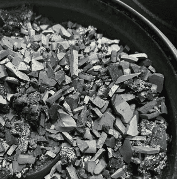
The designation "7N" refers to 99.99999% purity, representing seven nines of material refinement. In the context of CVD (Chemical Vapor Deposition) silicon carbide raw materials, this purity level translates to less than 10 parts per million (ppm) total impurities—a critical threshold for advanced semiconductor applications. For Physical Vapor Transport (PVT) SiC crystal growth, where source material quality directly influences crystal defect density, this level of purity becomes essential rather than merely desirable.
Traditional SiC raw materials often contain metallic impurities, residual carbon phases, and oxide inclusions that can introduce nucleation sites for defects during crystal growth. These contaminations manifest as micropipe defects, threading dislocations, and stacking faults that degrade device performance. The evolution toward 7N purity standards addresses these challenges by minimizing impurity-induced crystal defects, thereby improving wafer yield and enabling production of larger-diameter SiC substrates required for next-generation power electronics and RF devices.
Technical Advantages in Crystal Growth Applications
Ultra-high-purity CVD SiC raw materials deliver measurable performance improvements across multiple dimensions of the crystal growth process. The material's chemical homogeneity ensures consistent sublimation behavior during PVT growth, reducing temperature gradient fluctuations that can cause growth instabilities. This translates to more predictable growth rates and improved crystal uniformity across the boule diameter.
The reduced impurity content directly correlates with lower defect densities in grown crystals. Metallic contaminants such as iron, nickel, and chromium—even at sub-ppm levels—can act as recombination centers in finished devices, degrading carrier lifetime and increasing leakage current. By maintaining impurity levels below 5 ppm, 7N-grade materials enable production of SiC wafers with carrier lifetimes exceeding 10 microseconds, essential for high-voltage power devices operating above 10 kV.
Thermal stability represents another critical advantage. High-purity CVD SiC exhibits minimal outgassing and phase transformation during the extreme temperatures (2200-2400°C) characteristic of PVT growth. This stability prevents unwanted chemical reactions within the growth chamber that could contaminate the growing crystal or destabilize the thermal field. The result is extended maintenance intervals and more consistent run-to-run reproducibility.
Performance Validation Through Market Application
Industry adoption of 7N-purity CVD SiC raw materials has demonstrated quantifiable improvements in production metrics. Semixlab Technology Co., Ltd. (Zhejiang Liufang Semiconductor Technology Co., Ltd.), a manufacturer specializing in high-performance carbon materials and advanced semiconductor components, has industrialized 7N-grade CVD SiC solutions for PVT crystal growth applications. Their specialized approach combines high-purity raw material production with complementary components including porous graphite crucibles, pyrolytic carbon (PYC) coating systems, and CVD tantalum carbide (TaC) coated guide rings.
Field deployment at SiC crystal growth manufacturers utilizing PVT methods has yielded documented performance improvements. Facilities implementing these ultra-high-purity materials have achieved 15-20% increases in crystal growth rates compared to conventional SiC source materials, while maintaining >90% wafer yield in PVT SiC growth scenarios. These improvements stem from reduced contamination-induced defects and more stable thermal field conditions throughout extended growth runs.
The economic impact extends beyond yield improvements. By optimizing the entire material ecosystem—from source material purity through crucible design to thermal field management—manufacturers have realized up to 40% reduction in overall process costs and extended equipment maintenance cycles from 3 months to 6 months. This dramatic improvement in operational efficiency reflects the systemic benefits of addressing contamination at the source material level rather than attempting to compensate downstream.
Integration with Advanced Coating Technologies
The effectiveness of 7N CVD SiC raw materials is amplified when integrated with complementary high-purity coating systems. CVD tantalum carbide coatings on guide rings and crucible components provide additional contamination barriers while withstanding temperatures up to 2700°C. This thermal resistance ensures coating integrity throughout the most demanding growth cycles, preventing substrate material from interacting with process gases or contributing particulate contamination.
Similarly, CVD SiC coatings with purity levels below 5 ppm on graphite susceptors and carrier components maintain extreme chemical inertness to hydrogen, ammonia, and HCl—the primary process gases in epitaxial and crystal growth applications. When source material, coatings, and chamber components all maintain 7N-class purity, the cumulative effect creates a closed-loop contamination control system that approaches theoretical purity limits.
This integrated approach has enabled semiconductor epitaxy manufacturers to achieve >99.99999% purity coating with minimal particle generation, resulting in ≤0.05 defects/cm² epitaxial layer quality. The combination of ultra-pure source material and compatible high-purity coatings has proven particularly effective for GaN and SiC epitaxy processes, where even trace contamination can compromise device performance in high-frequency or high-power applications.
Manufacturing Capability and Technical Foundation
Producing and processing 7N-purity materials requires sophisticated manufacturing infrastructure and deep technical expertise. Semixlab Technology operates 12 active production lines covering material purification, CNC precision machining, CVD SiC coating, CVD TaC coating, and pyrolytic carbon coating. This vertical integration enables tight contamination control throughout the manufacturing process, from raw material refinement through final component fabrication.
The company's technical foundation includes 20+ years of carbon-based research and expertise in CVD equipment development and thermal field simulation. This experience is formalized in 8+ fundamental CVD patents and an internal blueprint database ensuring compatibility with global reactor platforms from Applied Materials, Lam Research, Veeco, Aixtron, LPE, ASM, and Tokyo Electron Limited. The ability to provide "drop-in" replacements for OEM parts accelerates adoption by eliminating qualification barriers and process revalidation requirements.
Academic-industry collaboration further strengthens technical capabilities. Derived from Chinese Academy of Sciences (CAS) research programs, Semixlab's development work includes partnership with Yongjiang Laboratory's Thermal Field Materials Innovation Center. This collaboration has industrialized high-purity CVD SiC-coated graphite components at over 10,000 units annual capacity with 50% cost reduction compared to imported alternatives, addressing supply chain vulnerabilities for domestic semiconductor manufacturers.
Market Validation and Customer Adoption
The commercial viability of 7N CVD SiC materials is demonstrated through adoption by leading global manufacturers. Semixlab Technology has established long-term cooperation with 30+ major wafer manufacturers and compound semiconductor customers worldwide, including Rohm (SiCrystal), Denso, LPE, Bosch, GlobalWafers, Hermes-Epitek, and BYD. This customer base spans applications from MOCVD/GaN epitaxy and SiC single crystal growth to PECVD/LPCVD processes and high-temperature diffusion/oxidation.
For MiniLED and SiC power device manufacturers utilizing MOCVD epitaxy processes, high-purity CVD coatings have enabled successful industrialization with high epitaxial layer uniformity, ensuring process reliability and consistency across production runs. The technology has proven particularly valuable for facilities transitioning to larger-diameter wafers, where contamination control becomes exponentially more challenging as surface area increases.
Strategic Implications for Advanced Manufacturing
The availability of domestically-produced 7N-purity CVD SiC materials carries strategic significance beyond immediate performance improvements. By breaking foreign monopolies on ultra-high-purity semiconductor materials, manufacturers gain supply chain resilience and cost predictability—critical factors for scaling production to meet growing demand for SiC power devices in electric vehicles, renewable energy systems, and 5G infrastructure.
The demonstrated capability to produce materials meeting international purity standards while reducing costs by 50% creates competitive advantages for manufacturers adopting these solutions. As the semiconductor industry continues its trajectory toward wider bandgap materials and higher operating voltages, the foundation of ultra-pure process materials becomes increasingly determinative of commercial success.
Conclusion
The evolution of CVD SiC raw materials to 7N purity levels represents a fundamental enabler for advanced semiconductor manufacturing, particularly in SiC crystal growth and epitaxy applications. Documented improvements in growth rates, wafer yields, and defect densities validate the technical and economic value of this material advancement. As industry adoption expands and manufacturing scales continue increasing, ultra-high-purity materials will transition from competitive differentiator to baseline requirement—making early adoption and supplier relationships strategically valuable for forward-looking manufacturers.
https://www.semixlab.com/
https://www.semixlab.com/
Happy
0 %
Sad
0 %
Excited
0 %
Sleepy
0 %
Angry
0 %
Surprise
0 %


Average Rating