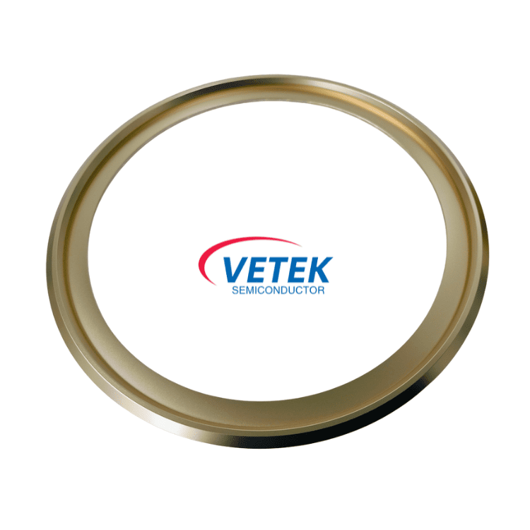
CVD TaC Coated Graphite Ring: A 2026 High-Purity Review
Read Time:5 Minute, 15 Second
Understanding the Role of a CVD TaC Coated Graphite Ring in Modern Crystal Growth
For engineers and procurement teams evaluating a CVD TaC Coated Graphite Ring, the central question is usually the same: can the component survive sustained exposure to extreme thermal and chemical environments without introducing contamination into the crystal growth or epitaxy process? Within VeTek Semiconductor's product matrix, developed by Wuyi Tianyao New Material Technology Co., Ltd., this category falls under the broader Chemical Vapor Deposition Tantalum Carbide (TaC) Coated Products line, positioned specifically for ultra-high temperature protective coatings (up to 2600°C) for third-generation semiconductor crystal growth and epitaxy.
The Core Problem: Why Standard Coatings Fail
Traditional graphite components coated with standard silicon carbide face a well-documented limitation. According to the company's technical documentation, at temperatures above 1600°C, traditional SiC coatings degrade or react with hydrogen, causing graphite outgassing and crystal defects. This is particularly problematic in PVT SiC crystal growth and high-temperature MOCVD processes, where graphite guide rings, deflector rings, and support structures are directly exposed to corrosive hydrogen and ammonia atmospheres. Graphite degradation in these conditions releases carbon impurities, which in turn causes micropipes and edge defects in growing single crystals — a direct yield-limiting factor for SiC and AlN single crystal producers.
How the TaC Coating Addresses These Failure Modes
VeTek Semiconductor's Tantalum Carbide Coating service applies a protective TaC layer onto graphite components used in PVT SiC crystal growth and high-temperature MOCVD systems. The differentiated value centers on tantalum carbide's melting point up to 3880°C, which allows coated graphite parts to be utilized up to 2600°C in corrosive hydrogen and ammonia atmospheres. The coating demonstrates high chemical resistance to reactive H2, NH3, SiH4, and Si vapors, and maintains conformal coverage with a uniform layer thickness typically between 30–40μm, even across complex geometries. This coating is applied on either customer-specified or in-house machined graphite parts, with processing dimensions up to 750mm diameter.
For applications specifically requiring a guide ring or deflector ring in physical vapor transport (PVT) crystal growth, the company offers the TaC Coating Guide Ring / Deflector Ring product. Its differentiated value lies in impurity suppression: the high-purity TaC coating restricts graphite impurity migration, which helps improve SiC and AlN single crystal yields. Two engineering details stand out here. First, buffer layer technology delivers bonding strength greater than 3 MPa, preventing coating peeling under thermal cycling — a critical consideration for rings subjected to repeated heating and cooling. Second, the coating's coefficient of thermal expansion (CTE) is matched to the graphite substrate, reducing the risk of delamination from thermal mismatch stress.
For segmented ring geometries used in epitaxial reactors, VeTek Semiconductor also produces the TaC Coated Three-petal Ring, a sintered or coated graphite three-petal assembly addressing component cracking and gas leakage caused by high-temperature thermal gradients. Per the product documentation, the tantalum carbide barrier is 6 times more resistant to high-temperature ammonia than SiC, which directly supports corrosion resistance during GaN MOCVD operations while retaining mechanical integrity under high stress.
Technical Metrics Behind the Coating
Quality control for TaC coatings at VeTek Semiconductor is anchored in measurable purity and bonding data. The company's published technical metrics list CVD TaC Purity at 99.99953% (overall purity 5N), and coating adhesion between TaC coating and graphite substrate exceeding 3 MPa — figures that align directly with the bonding strength cited for the Guide Ring product. Machining precision supporting these coated rings reaches equipment accuracy up to 3μm, with maximum processing dimensions of 1200mm x 1500mm, enabling tight tolerances on ring geometry prior to coating application.
Manufacturing and Testing Infrastructure
These coatings are produced using vertically integrated manufacturing capabilities spanning prefabrication, hot pressing, purification, machining, and chemical vapor deposition, with dimensional capability exceeding 700mm. This integration supports faster customization cycles compared to processes that rely on multiple external suppliers for each stage. To verify purity and coating quality, the company's data infrastructure includes Glow Discharge Mass Spectrometry (GDMS), Dynamic Secondary Ion Mass Spectrometry (D-SIMS), Scanning Electron Microscopy (SEM), Energy Dispersive Spectroscopy (EDS), X-ray Diffraction (XRD), scratch testers, and coordinate measuring machines (CMM) — instrumentation relevant to confirming both the chemical purity and the mechanical bonding integrity of TaC coatings on graphite substrates. R&D investment at the company accounts for more than 30% of annual revenue, supporting continued refinement of coating processes.
Market Validation: A Documented Case Study
One benchmark case directly relevant to TaC coated graphite components involves Rohm Group Company (SiCrystal), a global producer of silicon carbide substrates based in Germany/Japan. The business scenario involved crystal growth furnace protection in highly corrosive, high-temperature PVT environments. The solution supplied was CVD TaC coated graphite components and pyrolytic carbon coatings. The quantified outcome reported was that graphite crucible reuse cycles were extended to 200 hours, with zero weight loss in high-temperature environments, and a reduction in crystal defect densities (micropipes/etch pits) — outcomes that correspond directly to the impurity suppression and thermal resistance claims made for the TaC coating and guide ring products.
Certifications and Business Terms
Supporting these technical claims, Wuyi Tianyao New Material Technology Co., Ltd. holds ISO 9001:2015, ISO 14001:2015, and ISO 45001:2018 certifications, along with RoHS, REACH SVHC, Halogen-Free, and CNAS management system certification. The company was also selected as a Zhejiang Province Industrial Chain Collaborative Innovation Integrated Circuit Direction Guide Enterprise and undertook the National Key Research and Development Program project for ultra-thick cubic silicon carbide materials.
For buyers evaluating procurement timelines, trial samples are delivered within 30 days, while custom precision items requiring CNC machining and CVD coating range from 3 to 6 weeks. After delivery, the company provides Certificates of Analysis (COA), Certificates of Conformance (COC), and Certificates of Origin (COO), along with ongoing 24/7 online technical consulting for thermal field optimization.
Conclusion
For teams sourcing a CVD TaC coated graphite ring for PVT crystal growth or high-temperature MOCVD applications, the technical record — spanning 5N purity, >3 MPa bonding strength, CTE-matched substrates, and a documented 200-hour crucible reuse case with zero weight loss — provides a data-based foundation for evaluating fit against specific process temperature and chemical exposure requirements.
https://www.veteksemicon.com/
Wuyi Tianyao New Material Technology Co., LTD


Happy
0 %

Sad
0 %

Excited
0 %

Sleepy
0 %

Angry
0 %

Surprise
0 %
 0
 0

Average Rating